LTO, DOPED LTO, BPSG, BSG, AND PSG LPCVD
Low temperature oxides are used for sacrificial layers, diffusion masks, ion implant masks, etch masks, insulation, and passivation. These processes run at a much lower temperature (400 - 450 °C) than thermal oxidation and are thus compatible with more materials. The CVD film quality is correspondingly lower: lower dielectric strength, higher k, nonconformal step coverage, and hydrogen impurity incorporation that lowers density and increases HF etch rate. A post-deposition anneal increases the film density and makes the etch rate more uniform. Doping the oxide reduces its melting point for reflow, increases its etch rate (which makes it even more attractive as a sacrificial layer), and decreases the stress. Phosphorus can also getter contaminants like sodium.
PSG affects the properties of polysilicon grown on top of it. For a 605 °C polysilicon deposition, the orientation is (111) instead of (110) and the stress is considerably lower. Sandwiching a polysilicon layer between two PSG layers and annealing is a means of doping polysilicon while reducing its stress.
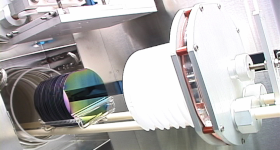
Silane spontaneously reacts with oxygen in the gas phase, so to avoid an unacceptably large concentration gradient down the process tube, separate distributed injectors are used to deliver the gases. A low-mass heater is required for good temperature control and caged wafer boats are required for good uniformity.
- Typical film thickness: 0.05 - 3 µm
- Refractive index at 550 nm / 1.45 - 1.47
- Batch Size: 25
- Deposition rate: 15 - 22.5 nm/min
- Gases: silane, oxygen, phosphine, and boron trichloride
- Uniformity: < 5%
- Dopant content: 6.5 - 7.0%
LPCVD Processes
- Silicon Carbide Devices
- Silicon Nitride Resonators
- Doped Silicon by LPCVD
- POLYSILICON LPCVD WITH SILANE (SiH4)
- POLYSILICON LPCVD WITH DISILANE (Si2H6)
- LTO, DOPED LTO, BPSG, BSG, AND PSG LPCVD
- HTO LPCVD
- TEOS LPCVD
- Silicon Nitride LPCVD
- Low-Stress Silicon Nitride LPCVD
- Stochiometric Silicon Nitride LPCVD
- Silicon Oxynitride (SiNxOy) LPCVD
- Silicon Germanium (Si-Ge) LPCVD
- SIPOS (Semi-Insulating Polycrystalline Silicon)
- Polycrystalline Silicon Carbide
- Epitaxial Silicon
- Nano Materials LPCVD


