Low-Stress Silicon Nitride LPCVD
Low stress nitride is performed at a high ratio of DCS to NH3 flow rates (typically ~ 6). The consequence of such silicon-enriched deposition is a very low tensile stress. The stress depends mainly on the gas mixing ratio and the process temperature. The processing pressure is typically a few Torr or lower. Increasing the pressure and the temperature increases the deposition but sacrifices the uniformity.
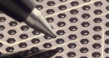
Applications: MEMS structures, diffusion barriers, passivation layers, oxidation masks, etch masks, ion implant masks, insulation, encapsulation, mechanical protection, gate dielectrics, optical waveguides, CMP and etch stop layers.
- Typical film thickness: 0.1 - 2 µm
- Refractive index at 550 nm / 2.0 - 2.3
- Batch Size: 50
- Deposition rate: 3 - 4.5 nm/min
- Gases: dichlorosilane, ammonia
- Uniformity: < 5%
- Stress: 50 - 300 MPa
- Deposition Temperature: 800 - 840 °C Flat
LPCVD Processes
- Silicon Carbide Devices
- Silicon Nitride Resonators
- Doped Silicon by LPCVD
- POLYSILICON LPCVD WITH SILANE (SiH4)
- POLYSILICON LPCVD WITH DISILANE (Si2H6)
- LTO, DOPED LTO, BPSG, BSG, AND PSG LPCVD
- HTO LPCVD
- TEOS LPCVD
- Silicon Nitride LPCVD
- Low-Stress Silicon Nitride LPCVD
- Stochiometric Silicon Nitride LPCVD
- Silicon Oxynitride (SiNxOy) LPCVD
- Silicon Germanium (Si-Ge) LPCVD
- SIPOS (Semi-Insulating Polycrystalline Silicon)
- Polycrystalline Silicon Carbide
- Epitaxial Silicon
- Nano Materials LPCVD