Amorphous Silicon by LPCVD
Polysilicon films are grown at 600-650 °C and amorphous silicon films (a-Si) are grown at 500-550 °C. Lower temperatures result in lower stress and smaller grain size. A post-growth anneal can be used to relieve film stress. Both large-grained and amorphous films have compressive stresses while smaller grains have tensile stresses. By alternating compressive and tensile layers, the overall stress can be kept low enough that a stress-relieving anneal is not required. Smaller grains have lower thermal conductivities and are etched faster by HF. Between 600 and 650 °C the film's orientation is predominantly (110), while at higher temperatures (100) dominates.
- Typical Film Thickness: 0.1 to 2 µm
- Batch Size: 50
- Deposition rate: 1-3 nm/min. (10 - 30 Å/min.)
- Deposition Temperature: 500 - 550 °C
- Refractive index at 550nm
- Uniformity: < 3% using 1 σ
- Gases: Silane SiH4
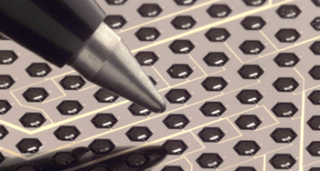
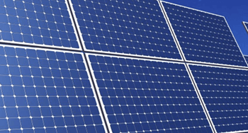
Applications: thin-film transistors for LCDs, thin-film photovoltaic solar cells
LPCVD Processes
- Silicon Carbide Devices
- Silicon Nitride Resonators
- Doped Silicon by LPCVD
- POLYSILICON LPCVD WITH SILANE (SiH4)
- POLYSILICON LPCVD WITH DISILANE (Si2H6)
- LTO, DOPED LTO, BPSG, BSG, AND PSG LPCVD
- HTO LPCVD
- TEOS LPCVD
- Silicon Nitride LPCVD
- Low-Stress Silicon Nitride LPCVD
- Stochiometric Silicon Nitride LPCVD
- Silicon Oxynitride (SiNxOy) LPCVD
- Silicon Germanium (Si-Ge) LPCVD
- SIPOS (Semi-Insulating Polycrystalline Silicon)
- Polycrystalline Silicon Carbide
- Epitaxial Silicon
- Nano Materials LPCVD