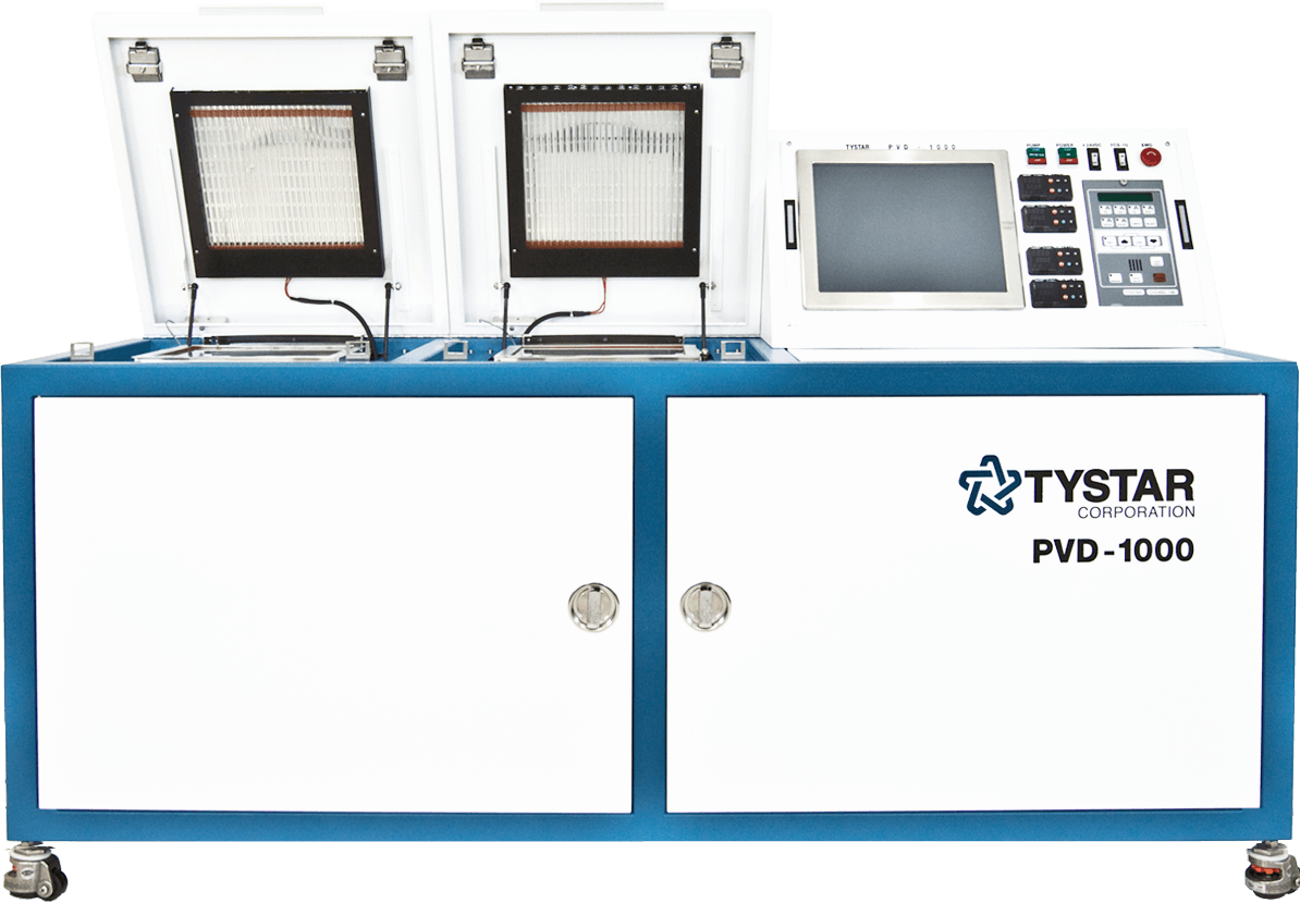
PHOTO-ENHANCED CHEMICAL VAPOR DEPOSITION REACTOR
The Tystar PVD 1000 Photo-Enhanced CVD Reactor uses ultraviolet light as an energy source for activating process gases for the deposition of dielectric films at low temperatures (<150 °C). Films of silicon-dioxide (SiO2), silicon nitride (Si3N4), silicon oxy-nitride (SiON) and others can be deposited. Minimal stress is observed in these films due to the low deposition temperature. Since the UV photon energy used does not ionize the process gases, no radiation damage from charged particles has been observed.
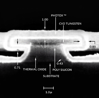
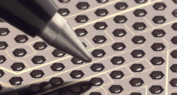
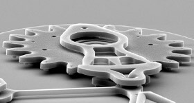
One of the characteristics of a good semiconductor film, alongside sparsity of pin holes, is conformal step coverage. A smooth and conformal film similar to the SiO2 film in the SEM image shown above ensures minimal electromigration and resistant pathways. This is one of the benefits of using a PVD-1000 system in thin film deposition.
The PVD 1000 deposited films offer excellent step coverage. The PVD 1000 system is available with single or dual-process chambers. The PVD 1000 reactor is used in a variety of applications for film deposition on "III/V" materials, such as gallium arsenide, indium antimonide and other materials that cannot tolerate higher deposition temperatures.